7 min read Maosheng Yang, Flemming Holtorf, and Frank Schäfer
From Optics Letter to Digital Twin: A Virtual Rebuild of the Taillaert 2004 Grating Coupler
A digital twin of the Taillaert 2004 grating coupler, built end to end by our AI agent and held to the paper's own quantitative claims at a verification and validation gate.
- digital twin
- lemma
- silicon photonics
On this page
At Axiomatic AI we use AI to build digital twins of physical systems and processes. A digital twin is only as useful as it is trustworthy, so our primary focus is verification and validation (V&V): every twin we ship is held against an independent source of truth, increasing justified confidence in the utility of the twin’s predictions, before anyone leans on it for engineering decisions.
This post illustrates our approach with an example from silicon photonics. The digital twin described hereafter was built by Lemma, our AI agent for scientists and engineers. Lemma read a paper about a given photonic device, drew up a plan for implementing a physics-based computational model capable of predicting the device’s key performance metrics, transformed this plan into a performant computational implementation by orchestrating domain-specific FDTD tooling (Tidy3D) to run the simulation on the cloud and turn the raw electromagnetic fields into the paper’s figures of merit. Lemma performed the workflow, and the results take the same quantitative checks into account that a photonics specialist would apply.
The device under consideration is a landmark silicon-photonics result: Taillaert, Bienstman & Baets, “Compact efficient broadband grating coupler for silicon-on-insulator waveguides” (Optics Letters, 2004). It tackles one of the archetypical problems in silicon photonics: getting light from an optical fiber into a 220-nm-thick silicon wire, where a ~10 µm fiber mode must meet a sub-micron-sized waveguide. Grating couplers solve this without polished facets and allow wafer-scale testing, but historically forced a tradeoff between coupling efficiency and broadband performance. The paper’s contribution was breaking that tradeoff, achieving sub-1 dB loss over a 35 nm band. In doing so it reports several quantitative results that a reproduction can be held against: peak efficiency, bandwidth, and minimum feature size.
The validation anchor
Trust in a digital twin does not come from a curve that looks plausible; it comes from a physics-based model reproducing specific, physically meaningful metrics that the original work reports. We use these metrics as the validation targets.
The paper decomposes coupling efficiency into three independent factors:
- — directionality: the fraction of radiated power sent up toward the fiber. A plain SOI grating leaks ~35% down into the substrate; a 2-pair Si/SiO₂ distributed Bragg reflector (DBR) below the buried oxide reflects that back up.
- — fiber-mode overlap: how well the radiated near-field matches the fiber’s Gaussian beam profile. A uniform grating radiates a one-sided decaying exponential, capping the overlap near 80%. Apodizing the grating, i.e., chirping the duty cycle so the local leakage traces a Gaussian, pushes this to ≈0.97.
- — lateral factor: the correction for treating a 3D device in a 2D simulation, ≈0.97.
This factorization allows for validating the computation factor by factor rather than only at a single headline number.
The role of AI in this exercise
Lemma planned and executed the reproduction as an autonomous workflow:
- Extract the architecture. From the paper’s text and figures: 220 nm Si core, 925 nm optimized buried oxide, index-matched top oxide, 8° fiber tilt, SMF-28 fiber (MFD 10.4 µm), 20-groove apodized grating, 30 nm minimum groove, 2-pair quarter-wave DBR.
- Synthesize the geometry. Turn the design vector
[period, chirp, α_max, z0, w0, t_box, etch]into physical groove widths via the apodization law and asin²duty-cycle inversion. - Orchestrate the solver. Build the 2D Tidy3D domain, place the mode source and flux/field monitors, launch the waveguide mode, and submit the run to the cloud.
- Post-process into the paper’s KPIs. Compute from up/down flux, from a tilted-Gaussian overlap integral against the FDTD near-field, assemble , and extract the peak and 1-dB bandwidth.
- Validate against the paper, factor by factor and headline to headline.
The workflow Lemma traverses to turn a paper into a digital twin of the device is illustrated below. The agent owns the whole loop, which terminates upon passing the V&V gate:
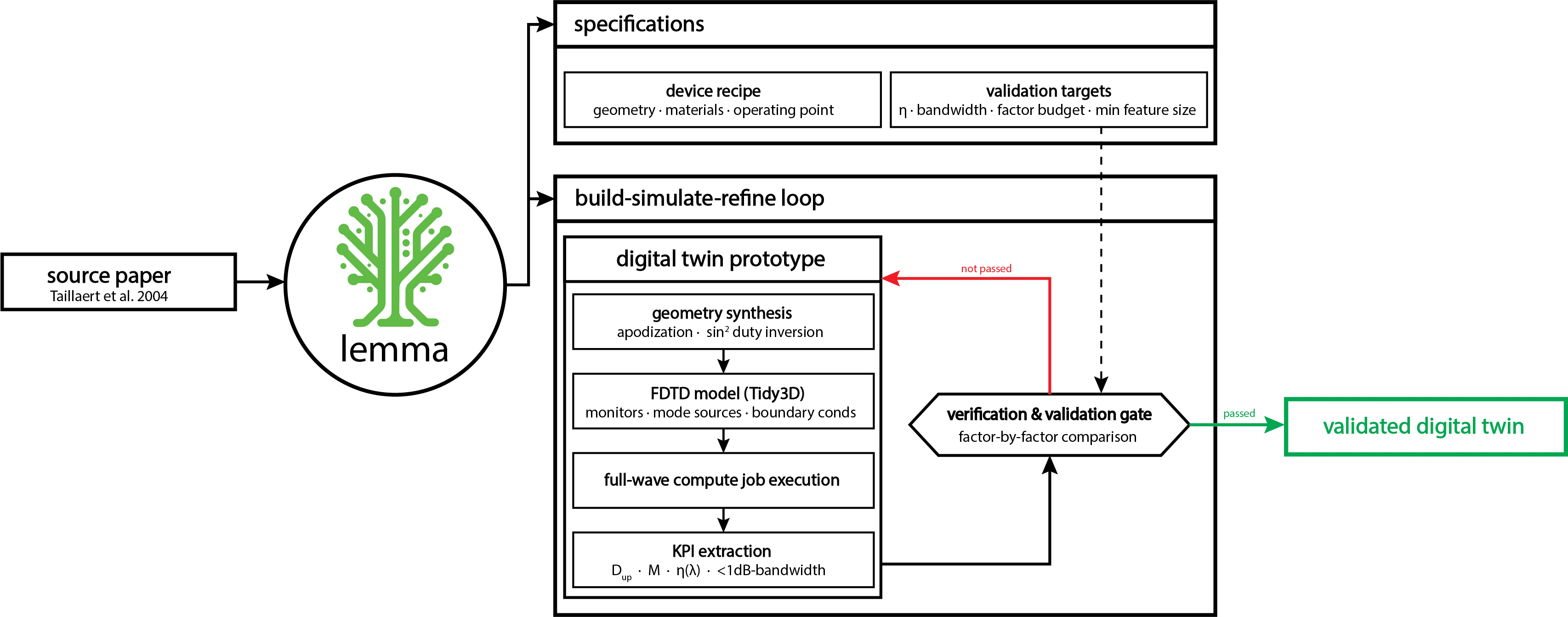
Figure: Lemma’s build-simulate-refine workflow: the source paper is read into two specification artifacts (the device recipe and the quantitative validation targets), after which the digital-twin prototype is synthesized, simulated with full-wave FDTD (Tidy3D), and reduced to KPIs, then held at a verification and validation gate that compares against all targets. A residual within tolerance yields the validated digital twin; otherwise the loop refines the geometry.
Two artifacts are extracted from the paper in parallel: 1. the recipe (what to build; here the device architecture) and 2. the validation targets (the quantitative criteria that the twin must reproduce). Both are deliberately kept separate so the targets are not contaminated by the modeling choices. Inside the build–simulate–reduce loop the digital twin is synthesized, simulated, and reduced to the validation targets. A V&V gate controls the iterative process: the model is accepted as a twin only when every factor agrees with the paper to within tolerance; a residual above tolerance returns the agent to the drawing board.
Output report: Verification & Validation
Lemma assembles its results into an output report that summarizes the underlying mathematical model, key assumptions, simulation results, and a factor-by-factor comparison against the paper. This report is intended for technical review and communication.
First, the model that was built. Lemma returns a visualization of the geometry and material stack: the 220 nm silicon core carrying the 20 apodized grooves, the buried oxide, and the two-pair Si/SiO₂ DBR mirror underneath it that recovers the downward-radiated light.
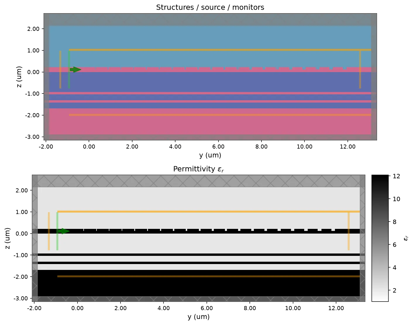
Figure: The digital twin as the solver sees it. Top: structures, source (green arrow) and monitors; bottom: the permittivity map used by the FDTD engine, showing the Si core, the buried oxide, and the DBR stack below it.
Next, the simulation results. The full-wave FDTD run of that geometry reproduces the near-unity broadband coupling the paper reported:
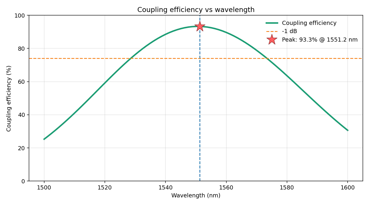
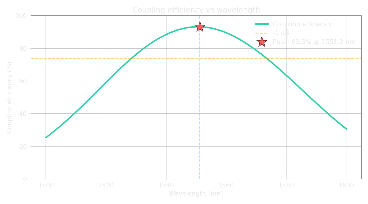
Figure: Independently computed fiber-coupling efficiency of the twin. The FDTD run peaks at 93.3% (−0.30 dB) at 1551 nm with a 1-dB bandwidth of ~45 nm.
Finally, the verdict. The table below shows the V&V gate checks for this study comparing Lemma’s independent FDTD twin against the paper’s EME results:
| Quantity | Taillaert 2004 (EME) | Lemma’s twin (FDTD) | Verdict |
|---|---|---|---|
| Peak efficiency η | 0.92 (−0.36 dB) | 0.933 (−0.30 dB) | ✓ |
| Directionality | ≈0.98 | 0.986 | ✓ |
| Fiber overlap | ≈0.97 | 0.975 | ✓ |
| Lateral factor | 0.97 | 0.97 | ✓ shared assumption |
| Back-reflection | “small” | 0.40% at peak | ✓ low |
| 1-dB bandwidth | 35 nm | 44.8 nm | ✓ exceeds |
| Min. groove width | 30 nm | 30 nm | ✓ |
The FDTD results agree closely with the published EME results. Because the two methods use different numerical formulations and implementations, this agreement provides a useful cross-check, although both models retain some shared physical assumptions. The residual differences are small and expected, e.g. a fraction-of-a-dB spread between two independent solvers on a re-derived geometry is exactly the agreement a validated twin should show.
An AI agent did the specialist work of building the model, and an independent validation provides evidence the model makes useful predictions.
This post describes a digital-twin reproduction of “Compact efficient broadband grating coupler for silicon-on-insulator waveguides” by Dirk Taillaert, Peter Bienstman, and Roel Baets (Optics Letters 29(23), 2004), built end-to-end by Lemma, Axiomatic AI’s agent. The original efficiency figures were obtained with the eigenmode-expansion method; the twin re-derives the geometry from the paper’s apodization recipe and validates it with independent full-wave FDTD. At Axiomatic AI we use AI to build digital twins of physical devices and processes with verification and validation anchors.